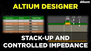
Media Summary: Multidisciplinary product creation powered by your unconstrained network. Work concurrently across design, sourcing, and ... Do you pour copper on your signal layers or not? Thank you very much Rick Hartley. Credits to Daniel Beeker, Lee Ritchy and ... Learn about material stackups and impedance

Pcb Stack Up And Controlled - Detailed Analysis & Overview

Multidisciplinary product creation powered by your unconstrained network. Work concurrently across design, sourcing, and ... Do you pour copper on your signal layers or not? Thank you very much Rick Hartley. Credits to Daniel Beeker, Lee Ritchy and ... Learn about material stackups and impedance Tips for designing with only two copper layers on a How do you intuitively engineer good impedance About This Video Learn how to design a 6-layer

You've completed your schematic design and are ready to begin the A brief look into what goes into making our Power planes can be incredibly useful in circuit board design, but if you put in on the wrong layer, it can cause a whole lot of ... In this Trace Talks snippet, Amit Bahl asks about KiCad's

Photo Gallery

PCB Stack-up and Controlled Impedance in Altium Designer
PCB Stack-Up and Build-Up - Phil's Lab #56
How to choose PCB stackup?
How to Decide on Your PCB Layer Ordering, Pouring and Stackup (with Rick Hartley)
Standard Stackup + Controlled Impedance Deep Dive
PCB Stackups & Impedance Control
How To Design a FLEX PCB | Stackup & Rules | Example in Altium
2-Layer PCB Design Tips - Phil's Lab #137
Understanding Layer Stackup and Impedance Control in OrCAD X
Intuitive Stack up Planning & Impedance Control
The Fundamentals of PCB Stackup Design
How to Design a 6-Layer PCB Stackup for Best Performance  #jlcpcb #pcbdesign #stackup
Sponsored
Sponsored
View Detailed Profile
PCB Stack-up and Controlled Impedance in Altium Designer

PCB Stack-up and Controlled Impedance in Altium Designer

Multidisciplinary product creation powered by your unconstrained network. Work concurrently across design, sourcing, and ...

PCB Stack-Up and Build-Up - Phil's Lab #56

PCB Stack-Up and Build-Up - Phil's Lab #56

What a

Sponsored
How to choose PCB stackup?

How to choose PCB stackup?

Why is the thickness of

How to Decide on Your PCB Layer Ordering, Pouring and Stackup (with Rick Hartley)

How to Decide on Your PCB Layer Ordering, Pouring and Stackup (with Rick Hartley)

Do you pour copper on your signal layers or not? Thank you very much Rick Hartley. Credits to Daniel Beeker, Lee Ritchy and ...

Standard Stackup + Controlled Impedance Deep Dive

Standard Stackup + Controlled Impedance Deep Dive

Multidisciplinary product creation powered by your unconstrained network. Work concurrently across design, sourcing, and ...

Sponsored
PCB Stackups & Impedance Control

PCB Stackups & Impedance Control

Learn about material stackups and impedance

How To Design a FLEX PCB | Stackup & Rules | Example in Altium

How To Design a FLEX PCB | Stackup & Rules | Example in Altium

If you have some tips for FLEX

2-Layer PCB Design Tips - Phil's Lab #137

2-Layer PCB Design Tips - Phil's Lab #137

Tips for designing with only two copper layers on a

Understanding Layer Stackup and Impedance Control in OrCAD X

Understanding Layer Stackup and Impedance Control in OrCAD X

Learn the essentials of layer

Intuitive Stack up Planning & Impedance Control

Intuitive Stack up Planning & Impedance Control

How do you intuitively engineer good impedance

The Fundamentals of PCB Stackup Design

The Fundamentals of PCB Stackup Design

Designing a

How to Design a 6-Layer PCB Stackup for Best Performance  #jlcpcb #pcbdesign #stackup

How to Design a 6-Layer PCB Stackup for Best Performance #jlcpcb #pcbdesign #stackup

About This Video Learn how to design a 6-layer

Multilayer PCB Manufacturing Process | Stack-Up, Production & Quality Control

Multilayer PCB Manufacturing Process | Stack-Up, Production & Quality Control

Ever wondered how multilayer

PCB Stack Up Factors to Consider

PCB Stack Up Factors to Consider

You've completed your schematic design and are ready to begin the

Understanding 2+n+2 Stackups in HDI Design

Understanding 2+n+2 Stackups in HDI Design

... click here: https://youtube.com/playlist?list=PL3aaAq2OJU5F4hyKgGyHKOfSIUU_hY_yv 2+N+2

PCB Materials + Stack up

PCB Materials + Stack up

A brief look into what goes into making our

How to Use Power Planes in Your PCB Stackup

How to Use Power Planes in Your PCB Stackup

Power planes can be incredibly useful in circuit board design, but if you put in on the wrong layer, it can cause a whole lot of ...

PCB Stack-Up Support and Other KiCad Advanced Features | Trace Talks EP 5

PCB Stack-Up Support and Other KiCad Advanced Features | Trace Talks EP 5

In this Trace Talks snippet, Amit Bahl asks about KiCad's

REDUCE EMI with PCB Design

REDUCE EMI with PCB Design

EMI,

Related Video Content

Printed circuit board - Wikipedia information

Printed circuit board of a DVD player Part of a 1984 Sinclair ZX Spectrum computer board, a printed circuit board,...

What is a PCB? A Beginner's Guide - nextpcb.com information

Discover what a PCB (Printed Circuit Board) is. Learn the basic anatomy, from the substrate and copper traces to the...

PCBs Explained: A Simple Guide to Printed Circuit Boards information

A PCB is a circuit board made from multiple layers of materials, arranged somewhat like a sandwich. The number of...

Circuit Board Components: Identification Guide & PCB Parts List information

Jul 31, 2025 · Discover common circuit board components, their functions, and how to identify them. Includes a PCB...

Home - PCB Bank information

PCB Bank offers a variety of checking accounts and savings accounts, digital banking and highly competitive rates on...