Media Summary: Increase the accuracy and efficiency of surface Stanford graduate school class CS230 Fall 2019 Project, by SCPD students, Jie and Chen, An Introduction to Electronics Systems Packaging by Prof. G.V. Mahesh, Department of Electronic system Engineering, IISc ...

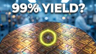
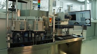
Wafer Defect Analysis Example - Detailed Analysis & Overview

Increase the accuracy and efficiency of surface Stanford graduate school class CS230 Fall 2019 Project, by SCPD students, Jie and Chen, An Introduction to Electronics Systems Packaging by Prof. G.V. Mahesh, Department of Electronic system Engineering, IISc ... Citable DOI: 10.5281/zenodo.10981906 Reuploaded due to YouTube error in audio/video sync in final 30 mins; original video ... Hello my name is adam faskowitz and i will be giving a Tech Talk: Darin Collins, director of metrology at Brewer Science, talks with Semiconductor Engineering about the cause of ...

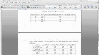
SmartDef3 software allows the users to analyze any type of Leo Pang, EVP at D2S, talks with Semiconductor Engineering about the problems of patterning at 40nm and below and how to ...

Photo Gallery

Wafer defect analysis example
Semiconductor wafer defect inspection and review system
Defect Rate in Semiconductors Wafers (2 Minutes)
Wafer Surface Defects Detection Using Deep Learning
Wafer Defect Inspection
MIMOS Failure Analysis - Wafer Level Testing
Wafer Map Failure Pattern Classification Using Deep Learning
Mod-02 Lec-07 Wafer fabrication, inspection and testing
Tutorial: Modelling Point Defects in Semiconductors with VASP (Audio Fix)
Lecture 32 (CHE 323) Semiconductor Manufacturing Yield
MIMOS Failure Analysis (Full Version)
Example of a design problem (Wafer Manufacturing System)
Sponsored
Sponsored
View Detailed Profile
Wafer defect analysis example

Wafer defect analysis example

Wafer defect analysis example

Semiconductor wafer defect inspection and review system

Semiconductor wafer defect inspection and review system

RWMAP is a powerful

Sponsored
Defect Rate in Semiconductors Wafers (2 Minutes)

Defect Rate in Semiconductors Wafers (2 Minutes)

...

Wafer Surface Defects Detection Using Deep Learning

Wafer Surface Defects Detection Using Deep Learning

Increase the accuracy and efficiency of surface

Wafer Defect Inspection

Wafer Defect Inspection

Wafer Defect Inspection

Sponsored
MIMOS Failure Analysis - Wafer Level Testing

MIMOS Failure Analysis - Wafer Level Testing

Wafer

Wafer Map Failure Pattern Classification Using Deep Learning

Wafer Map Failure Pattern Classification Using Deep Learning

Stanford graduate school class CS230 Fall 2019 Project, by SCPD students, Jie and Chen,

Mod-02 Lec-07 Wafer fabrication, inspection and testing

Mod-02 Lec-07 Wafer fabrication, inspection and testing

An Introduction to Electronics Systems Packaging by Prof. G.V. Mahesh, Department of Electronic system Engineering, IISc ...

Tutorial: Modelling Point Defects in Semiconductors with VASP (Audio Fix)

Tutorial: Modelling Point Defects in Semiconductors with VASP (Audio Fix)

Citable DOI: 10.5281/zenodo.10981906 Reuploaded due to YouTube error in audio/video sync in final 30 mins; original video ...

Lecture 32 (CHE 323) Semiconductor Manufacturing Yield

Lecture 32 (CHE 323) Semiconductor Manufacturing Yield

Semiconductor Manufacturing: Yield and

MIMOS Failure Analysis (Full Version)

MIMOS Failure Analysis (Full Version)

MIMOS Failure

Example of a design problem (Wafer Manufacturing System)

Example of a design problem (Wafer Manufacturing System)

We present an

Behind the Scenes: How to Build the Wafer Pattern Classification Machine Learning App

Behind the Scenes: How to Build the Wafer Pattern Classification Machine Learning App

Hello my name is adam faskowitz and i will be giving a

Defect Reduction At 7/5nm

Defect Reduction At 7/5nm

Tech Talk: Darin Collins, director of metrology at Brewer Science, talks with Semiconductor Engineering about the cause of ...

Semiconductor Yield Management and Defect Analysis (9 Minutes)

Semiconductor Yield Management and Defect Analysis (9 Minutes)

Semiconductor Yield Management and

Wafer Supervised Inspection - SmartDef3

Wafer Supervised Inspection - SmartDef3

SmartDef3 software allows the users to analyze any type of

Large Wafer Analysis System

Large Wafer Analysis System

HORIBA Scientific's New Large

Promicron high-speed epi wafer inspection and ADC, counting and classifying defects defect map

Promicron high-speed epi wafer inspection and ADC, counting and classifying defects defect map

Promicron high-speed epi

Wafer Plane Analysis (2015)

Wafer Plane Analysis (2015)

Leo Pang, EVP at D2S, talks with Semiconductor Engineering about the problems of patterning at 40nm and below and how to ...

Wafer Map Failure Pattern Classification Using Deep Learning

Wafer Map Failure Pattern Classification Using Deep Learning

Stanford graduate school class CS230 Fall 2019 Project, by SCPD students, Jie and Chen,

Related Video Content

Wafer (electronics) - Wikipedia information

The wafer serves as the substrate for microelectronic devices built in and upon the wafer. It undergoes many...

WAFER Definition & Meaning - Merriam-Webster information

4 days ago · : a thin disk or ring resembling a wafer and variously used (as for a valve or diaphragm)