Media Summary: Hello my name is adam faskowitz and i will be giving a tutorial on how to use tibco's Reference Number: 1982 Title: Development of Intelligent We present an example where the manager of a
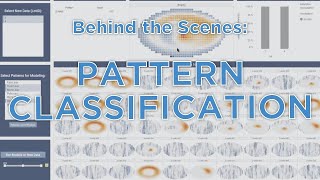
Wafer Map Failure Pattern Classification - Detailed Analysis & Overview
Hello my name is adam faskowitz and i will be giving a tutorial on how to use tibco's Reference Number: 1982 Title: Development of Intelligent We present an example where the manager of a Applied has the industry's broadest suite of materials capabilities for fabricating devices on semiconductor What is the process by which silicon is transformed into a semiconductor chip? As the second most prevalent material on earth, ... Contains explanation of CNN & Random Forest for semiconductor
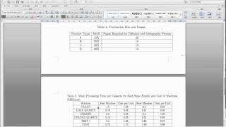
If you have gotten stuck during import with the message that the grids don't make sense or that the grids are not working then this ... 298B Group5 Used WM811K and WM38 dataset. Merged them and annotated the Two Dimensional Principal Component Analysis Based Convolutional Autoencoder for Introduction to Double Patterning which is used extensively for printing transistors and other features in front end of line (FEOL) ...