Media Summary: Increase the accuracy and efficiency of surface This video provides an overview of the data processes involved VISOR® Solar Vision sensor for automatic

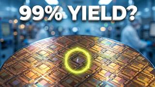
Smart Wafer Defect Detection Using - Detailed Analysis & Overview

Increase the accuracy and efficiency of surface This video provides an overview of the data processes involved VISOR® Solar Vision sensor for automatic Analyzing tens of thousands of images and video frames AI & Manufacturing "LaserSKI: Object Detection for Stanford graduate school class CS230 Fall 2019 Project, by SCPD students, Jie and Chen,

Reference Number: 1982 Title: Development of 298B Group5 Used WM811K and WM38 dataset. Merged them and annotated the Automated correctness checking of a simple assembly - Everyone knows how hard it is to find a needle

Photo Gallery

Smart Wafer Defect Detection using Lightweight CNN and Classical Filtering
Defect Rate in Semiconductors Wafers (2 Minutes)
Wafer Surface Defects Detection Using Deep Learning
Generative AI - How it Works for Defect Detection
VISOR® Solar Vision sensor for automatic detection of wafer and cell geometry - SensoPart
Hitachi Image Based Inspections: Defect Detection of Infrastructure Assets using AI-based Automation
LaserSKI: Object Detection for Defect Detection in Semiconductors | William Clemens
Wafer defect analysis example
Wafer Map Failure Pattern Classification Using Deep Learning
Moving Defect Detection And Classification To The Edge
Development of Intelligent Wafer Defects Classification System using Optimized Deep Learning Model
Semiconductor wafer defect inspection and review system
Sponsored
Sponsored
View Detailed Profile
Smart Wafer Defect Detection using Lightweight CNN and Classical Filtering

Smart Wafer Defect Detection using Lightweight CNN and Classical Filtering

Smart Wafer Defect Detection using

Defect Rate in Semiconductors Wafers (2 Minutes)

Defect Rate in Semiconductors Wafers (2 Minutes)

Defect

Sponsored
Wafer Surface Defects Detection Using Deep Learning

Wafer Surface Defects Detection Using Deep Learning

Increase the accuracy and efficiency of surface

Generative AI - How it Works for Defect Detection

Generative AI - How it Works for Defect Detection

This video provides an overview of the data processes involved

VISOR® Solar Vision sensor for automatic detection of wafer and cell geometry - SensoPart

VISOR® Solar Vision sensor for automatic detection of wafer and cell geometry - SensoPart

VISOR® Solar Vision sensor for automatic

Sponsored
Hitachi Image Based Inspections: Defect Detection of Infrastructure Assets using AI-based Automation

Hitachi Image Based Inspections: Defect Detection of Infrastructure Assets using AI-based Automation

Analyzing tens of thousands of images and video frames

LaserSKI: Object Detection for Defect Detection in Semiconductors | William Clemens

LaserSKI: Object Detection for Defect Detection in Semiconductors | William Clemens

AI & Manufacturing "LaserSKI: Object Detection for

Wafer defect analysis example

Wafer defect analysis example

Wafer defect analysis example

Wafer Map Failure Pattern Classification Using Deep Learning

Wafer Map Failure Pattern Classification Using Deep Learning

Stanford graduate school class CS230 Fall 2019 Project, by SCPD students, Jie and Chen,

Moving Defect Detection And Classification To The Edge

Moving Defect Detection And Classification To The Edge

The number of

Development of Intelligent Wafer Defects Classification System using Optimized Deep Learning Model

Development of Intelligent Wafer Defects Classification System using Optimized Deep Learning Model

Reference Number: 1982 Title: Development of

Semiconductor wafer defect inspection and review system

Semiconductor wafer defect inspection and review system

RWMAP is a powerful

WBM Defect Classification Using Custom YOLOV5 Model

WBM Defect Classification Using Custom YOLOV5 Model

298B Group5 Used WM811K and WM38 dataset. Merged them and annotated the

Wafer Defect Inspection

Wafer Defect Inspection

Wafer Defect Inspection

SmartDEF3 – Wafer Inspection & Automated Defect Clustering Workflow

SmartDEF3 – Wafer Inspection & Automated Defect Clustering Workflow

In

Wafer Map Failure Pattern Classification Using Deep Learning

Wafer Map Failure Pattern Classification Using Deep Learning

Stanford graduate school class CS230 Fall 2019 Project, by SCPD students, Jie and Chen,

Surface Defect Detection Using Autoencoder — Working Demo

Surface Defect Detection Using Autoencoder — Working Demo

Automated correctness checking of a simple assembly -

Taking a closer look at a semiconductor wafer using ultrafast lasers!

Taking a closer look at a semiconductor wafer using ultrafast lasers!

Everyone knows how hard it is to find a needle

video4

video4

Wafer Defect Detection

Wafer defect localization and classification using deep learning techniques

Wafer defect localization and classification using deep learning techniques

In

Related Video Content

SMART criteria - Wikipedia information

SMART is a mnemonic acronym used to establish criteria for goals and objectives that are specific, measurable,...

SMART information

At our core, we offer a student management software system which has been web-based for almost 20 years. This means...

The Ultimate Guide to S.M.A.R.T. Goals – Forbes Advisor information

Jun 2, 2025 · Fortunately, S.M.A.R.T. (specific, measurable, achievable, relevant and time-bound) goals can help all...

Log In | Smartsheet information

Log in to Smartsheet to access your workspace and collaborate on projects. Sign in with your email, Google, Apple,...

SMART Goal - Definition, Guide, and Importance of Goal Setting information

Jun 16, 2020 · A SMART goal is used to help guide goal setting. SMART is an acronym that stands for Specific,...